Day 1 :
Keynote Forum
Dan Botez
University of Wisconsin-Madison, USA
Keynote: High-internal-efficiency quantum cascade lasers: the road to mid-infrared lasers of 40% CW wall-plug efficiency
Time : 09:30-10:00

Biography:
Dan Botez is Philip Dunham Reed Professor in the Department of Electrical and Computer Engineering at University of Wisconsin (UW) - Madison. In 1976, he obtained a PhD degree in Electrical Engineering from University of California, Berkeley. He has carried out and led research in semiconductor lasers at RCA Labs, Princeton, NJ and TRW Research Center, Redondo Beach, CA before joining, in 1993, the faculty at UW-Madison. His research interests lie in three areas of semiconductor-laser physics: high-power, coherent edge-emitting lasers; high-power, coherent grating-coupled surface-emitting lasers; and quantum cascade lasers. The first two are based on one- and two-dimensional, high-index-contrast, photonic-crystal structures, respectively, for insuring both long-range spatial coherence and stable operation under continuous-wave (CW) driving conditions. The third involves electron transitions between the sub-bands of multi-quantum-well structures and is focused on achieving high-efficiency CW operation in the mid-infrared wavelength range: 3-10 microns, via multi-dimensional conduction-band engineering
Abstract:
The internal efficiency hi of quantum cascade lasers (QCLs) is the factor in the expression for the external differential efficiency that encompasses all differential carrier-usage (i.e., the injection efficiency) and lasing-photon-transition efficiencies. For conventional QCLs the hI values have been found to be rather low: 50-60% in the 4.5-6.0 μm wavelength range and 57-67% in the 7-11 μm wavelength range; with, until recently, no clear explanation why that was the case. With the advent of combining carrier-leakage suppression with fast, efficient carrier extraction out of the active regions of QCLs, the hi values have steadily increased and are approaching their fundamental upper limit of ~ 90% for mid-infrared (IR)-emitting devices. We will review the developments that led to high hi values throughout the mid-IR wavelength range. Conduction-band engineering has led to the so-called step-taper active-region (STA) QCLs which have provided hi values 30-50% higher than in conventional QCLs over both the 4.5-6.0 μm and 7-11 μm wavelength ranges. A record-high, single-facet, continuous-wave (CW) power, for 8.0 μm-emitting QCLs, of 1.0 Watt has been achieved from STA-type QCLs. Furthermore, the recognition that the fundamental limit for hi (i.e., 90%) is 34% higher than the hi value employed a decade ago when determining the fundamental limit for the wall-plug efficiency of mid-IR QCLs, has led to the realization that wall-plug efficiencies ≥ 40% can be achieved for 4.5-5.0 μm-emitting QCLs. The practical benefits of achieving such high performance from mid-IR emitting semiconductor lasers will be discussed as well.
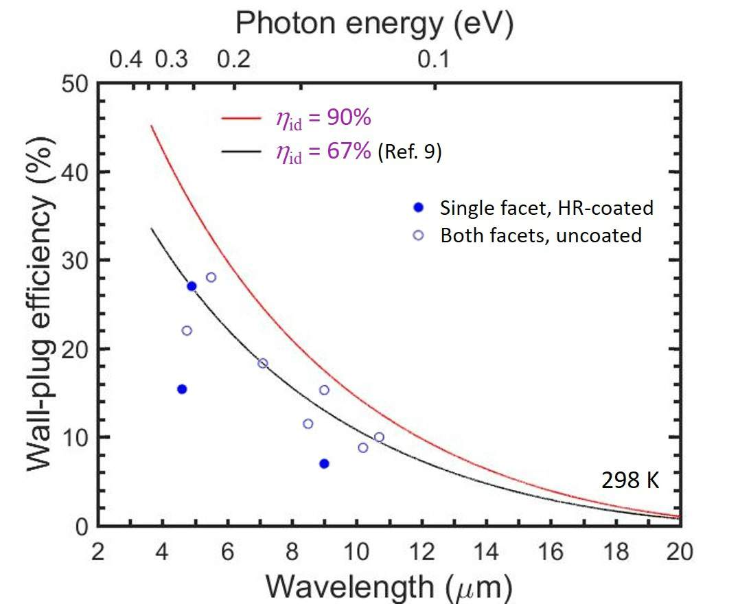
Wall-plug-efficiency fundamental limits for mid-infrared-emitting QCLs
Recent Publications
- Kirch J et al (2016) 86% internal differential efficiency from 8-9 µm-emitting, step-taper active-region quantum cascade lasers. Optics Express 24: 24483-24494.
- Botez D, Chang C-C, Mawst L J (2016) Temperature sensitivity of the electro-optical characteristics for mid-infrared-emitting quantum cascade lasers. J. Phys. D: Applied Physics 49: 043001.
- Botez D et al. (2013) Multidimensional conduction-band engineering for maximizing the continuous-wave (cw) wallplug efficiencies of mid-infrared quantum cascade lasers. IEEE Journal Selected Topics in Quantum Electronics 19 (4): 1200312.
- Kirch J et al. (2012) Tapered active-region quantum cascade lasers for suppression of carrier-leakage currents. Electron Lett. 48: 234.
5. Botez D et al. (2010) Temperature dependence of the key electro-optical characteristics for mid-infra-red emitting quantum cascade lasers. Applied Physics Letters 97: 071101.
Keynote Forum
Manyalibo J Matthews
Lawrence Livermore National Laboratory, USA
Keynote: Understanding laser materials processing: the dichotomy between laser damage and laser machining
Time : 10:00-10:30

Biography:
Manyalibo J Matthews currently serves as Deputy Group Leader in the Optical Materials and Target Science group in MSD. He holds a PhD in Physics from MIT and a BS in Applied Physics from UC Davis. His research interests at LLNL include novel applications in laser-assisted material processing (e.g. metal additive manufacturing, laser-based CVD, nano-coarsening of metal films, non-contact laser polishing of glass), optical damage science, vibrational spectroscopy and in-situ optical characterization of transient processes. Prior to LLNL, he was a Member of Technical Staff at Bell Labs and worked on materials characterization of optical devices using novel spectroscopic techniques, stress-induced birefringence management in planar optical devices and research in advanced broadband access networks. He is a Fellow of the Optical Society of America.
Abstract:
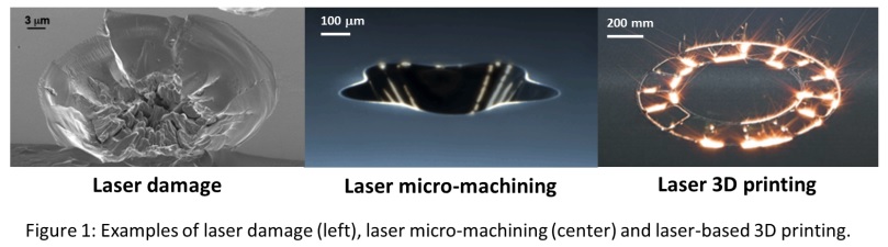
In the decades since the invention of the laser, new applications and discoveries in materials science have continued year after year as laser sources evolve and more areas of research exploit them. The transformation of materials using focused, high irradiance laser beams fundamentally involves multiple physical phenomena such as optical absorption, heat transport, structural mechanics and material phase transitions. For example, nonlinear absorption of nanosecond pulsed laser light can lead to a nano-scale thermal runaway effects and subsequent damage, which can be detrimental in the operation of high power laser systems. On the other hand, laser processing of materials often involves ablative removal of material or transformations which rely on efficient coupling of laser energy into a work piece. In both cases, understanding laser-material interactions is essential for the optimization of the high power optical system design. In this talk, we will present a few examples of high photon flux laser material processing, using both experiment and finite element modeling to understand energy deposition, heat transport and material transformation. Specifically, we will explore the conditions which bring about optical damage in ultraviolet Q-switched laser optics and compare these conditions to those used in typical microscale laser materials processing technologies. Among the laser processing techniques discussed, we will focus on microsecond-pulsed, resonant IR laser heating for laser micro-machining and metal powder bed additive manufacturing (3D printing). We will discuss how our results can be used to elucidate material behavior, optimize processing and develop new technologies based on laser modified materials.
Recent Publications
- C A R Chapman, L Wang, J Biener, E Seker, M M Biener, and M J Matthews (2016) Engineering on-chip nanoporous gold material libraries via precision photothermal treatment. Nanoscale. 8:785-795.
- M J Matthews, G Guss, S A Khairallah, A M Rubenchik, P J Depond and W E King (2016) Denudation of metal powder layers in laser powder bed fusion processes. Acta Materialia. 114:33-42.
- M J Matthews, S T Yang, N Shen, S Elhadj, R N Raman, G Guss, I L Bass, M C Nostrand and P J Wegner (2015) Micro-shaping, polishing, and damage repair of fused silica surfaces using focused infrared laser beams. Advanced Engineering Materials. 17:247-254.
- J H Yoo, J B In, I Sakellari, R N Raman, M J Matthews, S Elhadj, C Zheng and C Grigoropoulos (2015) Directed dewetting of amorphous silicon film by a donut-shaped laser pulse. Nanotechnology 26: 165303.
- M J Matthews (2015) Simulating laser-material interactions, Laser Focus World 51: 33-38.
Keynote Forum
Shien-Kuei Liaw
National Taiwan University of Science and Technology, Taiwan
Keynote: WDM bidirectional optical wireless communications
Time : 10:50-11:20

Biography:
Shien-Kuei Liaw received Double Doctorate from National Chiao-Tung University in Photonics Engineering and from National Taiwan University in Mechanical Engineering, respectively. He joined the Chunghua Telecommunication, Taiwan, in 1993. Since then, he has been working on Optical Communication and Fiber Based Technologies. He joined the Department of Electronic Engineering, National Taiwan University of Science and Technology (NTUST) in 2000. He has ever been Director of the Optoelectronics Research Center and the Technology Transfer Center, NTUST. He was a Visiting Researcher at Bellcore (now Telcordia), USA for six months in 1996 and a visiting Professor at University of Oxford, UK for three months in 2011. He owned six US patents, and authored or coauthored for 250 journal articles and international conference presentations. He earned many domestic honors and international honors. He has been actively contributing for numerous conferences as a conference chair, technical program chair, organizing committee chair, steering committee and/or keynote speaker. He serves as an Associate Editor for Fiber and Integrated Optics. Currently, he is a Distinguished Professor of National Taiwan University of Science and Technology (NTUST), Vice President of the Optical Society (OSA) Taiwan Chapter and Secretary-General of Taiwan Photonic Society. His research interests are in Optical Sensing, Optical Communication and Reliability Testing.
Abstract:
In this talk, high-speed free space optics communication (FSO) technologies will be reviewed and introduced. Then we will design and demonstrate two proposed FSO schemes. The first scheme is bi-directional short-range free-space optical (FSO) communication with 2x4x10 Gb/s capacity in wavelength division multiplexing (WDM) channels short transmission distance. The single-mode-fiber components are used in the optical terminals for both optical transmitting and receiving functions. The measured power penalties for bi-directional, four-channel WDM FSO communication are less than 0.8 dB and 0.2 dB, compared with the back-to-back link and uni-directional transmission system, respectively. The second scheme is hybrid optical fiber and FSO link in outdoor environments such as cross bridge or inter-building system. A sensor head is used for monitoring the condition of bridge, and in the case of the bridge being damaged the transmission path could be changed from fiber link to FSO link to ensure data link connectivity. In both cases, the single-mode-fiber (SMF) components are used in the optical terminals for both optical transmitting and receiving functions. The influences of environmental factor including window glasses, air turbulence and rainfall will also be addressed. The colorless and colored window glasses introduce losses under various incident angles, but did not induce substantial power penalties. The air turbulence induces extra transmission loss and instability in the received power. Raindrops are the most influential environmental factor. The bit error rate (BER) test shows that raindrops result in a seriously impaired BER to interrupt the transmission instantaneously. After appropriate performance improvement, these proposed transmission structures show potential applications for outdoor transmission under various natural weather conditions.
Keynote Forum
Carl C Jung
CCJ Software, Germany
Keynote: Twisted and turned layers – no problem for ITE (Immersion Transmission Ellipsometry)
Time : 11:20-11:50

Biography:
Carl C Jung has his expertise in finding mathematical models for engineering, physical and physical chemistry questions and implementing them in evaluation and simulation software. His way led from amperometric biosensors (Cambridge University, UK), via biophysics employing florescence (Max Planck Institute, Frankfurt a M) to display technology and ellipsometry (IDM, Berlin and Potsdam). Here the presented topic was generated. Thereafter he returned to biophysics and fluorescence (Bayreuth University), and after one year in research management (Fraunhofer, Munich) he finally performed theoretical and experimental studies on the heating of bond wires used in integrated circuits by electronic engineers (Robert Bosch Center for Power Electronics, Reutlingen).
Abstract:
If looking at optically thin layers or thin films with an anisotropic structure, the main applications of such films are in display technology. There are different ways, such layers can be used: as polarisers, if absorbing, as retarders, if transparent, as photo-alignment films, if very thin and with a specific surface, that can be used to align other attaching films during an annealing step in fabrication. Of course, the optical properties of the resulting display depend on the quality of the layers used to produce it. Therefore, we developed a new method, which can very accurately determine the three-dimensional refractive index and its orientation in a thin layer. Even films, whose properties vary in the direction perpendicular to the film plane, can be studied with success. We employed a combination of transmission in two different media - immersion transmission ellipsometry and reflection ellipsometry at one single wavelength. Ellipsometry is the measurement of the alteration of the polarization state of light transmitted or reflected by the layer or film studied. The accuracy of the method was very high compared to conventional reflection ellipsometry in only one medium. If compared to combined transmission and reflection measurements in air, we also reached a drastic improvement. The method of immersion transmission ellipsometry is a significant step forward in the development of non-destructive optical characterization methods for thin films with complex anisotropic structure.
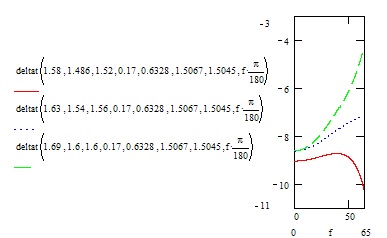
Figure 1: Three normally indistinguishable sets of data can be expanded by immersion transmission ellipsometry. Depicted is the ellipsometric parameter Δ measured in transmission under immersion. The first 3 figures are the refractive indices of the film. Then wavelength in µm, and immersion and substrate index follow.
- Jung C, Stumpe J (2015) Immersion transmission ellipsometry (ITE) for the determination of orientation gradients in photoalignment layers. Appl. Phys. B DOI 10.1007/s00340-013-5729-2.
- Jung C, Stumpe J (2005) Immersion transmission ellipsometry (ITE) – a new method for the precise determination of the 3D indicatrix of thin films. Appl. Phys. B 80:231-238.
- Jung C, Stumpe J, Peeters E, van der Zande B (2005) A novel way for the full characterisation of splayed retarders using the Wentzel-Kramers-Brillouin (WKB) method. Jpn. J. Appl. Phys. 44: 4000-4005.
Keynote Forum
Fabienne Michelini
Aix Marseille University, France
Keynote: Energy transfer dynamics in molecular junctions under ultra-short excitation pulses from non-equilibrium Green’s function formalism
Time : 11:50-12:20

Biography:
Fabienne Michelini has worked on the theoretical/numerical building of empirical models within the k·p method to understand the electronic properties of realistic condensed-matter systems. In parallel, she has gained a great expertise in high performance computing for large-scale numerical problems. For the last years, she has investigated the transport properties of opened quantum structures for novel nanodevices using effective methods within the Green function formalism. She is now focusing on time-dependent and non-linear regimes of nanosystems interacting with light for optoelectronic and thermoelectric applications at the nanoscale.
Abstract:
The problem of energy transfer is emerging as one of the most crucial issues of our occidental societies. At a fundamental level, how energy flows at the nanometre scale is gaining specific interests due to its implications in both alternative energy production and basics of quantum thermodynamics. The nature of our work is hence two-fold. In the first part, we provide a definition of energy current operator in the Heisenberg representation, while discussing certain conditions which an operator shall fulfill. The obtained expression is applicable to non-stationary as steady-state situations. We implement this definition to derive time-dependent energy current using non-equilibrium Green’s function formalism, which represents a suitable approach for calculating measurable quantities in opened nanosystems. The second part applies these developments to molecular junctions sandwiched in between two thermal reservoirs. Molecular electronic devices are indeed a promising alternative to standard electronic switches due to their fast response on the picosecond time scale. Here, the approach is used for the study of molecular junctions subjected to ultra-short excitation pulses. We thus analyze the electronic energy fluxes across the molecular junction engendered by femtosecond laser pulses. Our numerical implementation enables us to correlate the time-dependent energy current to the underlying intra-molecular dynamics, with special attention paid to the impacts of intra-molecular coupling and incoherence on the energy transfer time-resolved measurables.
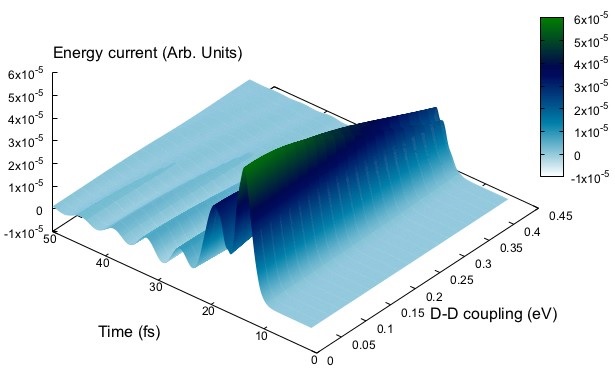
Figure 1: We consider a junction made of two donors (D) that interact with light and an acceptor (A), the whole is in contact with tow thermal reservoirs. Effects of the intra-molecular D-D coupling on the time-resolved energy current flowing from D to A during a 30 fs laser pulse
Recent Publications
-
Michelini F, Crépieux A, Beltako K (2017) Entropy production in photovoltaic-thermoelectric nanodevices from the non- equilibrium Green’s function formalism, J. Phys.: Condens. Matter 29: 175301.
- Beltako K, Cavassilas N, Michelini F (2016) State hybridization shapes the photocurrent in triple quantum dot nanojunctions, Appl. Phys. Lett. 109: 073501.
- Crépieux A, Michelini F (2015) Mixed, charge and heat noises in thermoelectric nanosystems, J. Phys.: Condens. Matter 27: 015302.
- Berbezier A, Autran JL, Michelini F (2013) Photovoltaic response in a resonant tunneling wire-dot-wire junction, Appl. Phys. Lett. 103: 041113.
- Crépieux A, Simkovic F, Cambon B, Michelini F (2011), Enhanced thermopower under a time-dependent gate voltage, Phys. Rev. B 83: 153417.
Keynote Forum
Shao-Wei Wang
Chinese Academy of Sciences, China
Keynote: Integrated narrow bandpass filters array for miniature spectrometer
Time : 00

Biography:
Shao-Wei Wang received his Ph.D. (2003) degree in microelectronics and solid state electronics from Shanghai Institute of Technical Physics, Chinese Academy of Sciences, China. He is a professor of the institute and works at National Laboratory for Infrared Physics from 2010. His research interests include artificial photonic structure and devices, such as interaction between high-Q optical cavity and low-dimensional materials, integrated-cavities for miniature spectrometers, solar selective absorbers, metamaterial polarizers, and optical thin films. He has published more than 50 research papers and authorized one US patent. He got LU JIAXI Young talent award (2009), RAO YUTAI basic optical award (2007) , National Natural science award (2014, 4th principal achiever), National Technological Invention Award (2011, 5th principal achiever), Shanghai Technological Invention Award (2010, 7th principal achiever), Shanghai Natural science award (2007, 5th principal achiever), etc.
Abstract:
Compact, lightweight, and rigid miniature spectrometers without moving parts are needed for a wide variety of applications, including space applications, where every inch of payload counts. Miniaturization increases the portability and paves the way for making in situ spectral measurements for daily life of Food-safety and health etc. It also eases the integration of microspectrometers and miniature spectrometers into other technologies, such as microelectronics, and helps to realize lab-on-a-chip devices.
It attracts many research interests in recent years. There are many novel wavelength devision approaches have been proposed for miniature spectrometers, such as colloidal quantum dot spectrometer and disordered photonic chip. The optical filter array is one of the most important components in wavelength-division multiplexing, multispectral devices, and parallel array optics, which are widely used in communication and electrooptical systems.
We proposed and realized the concept of integrated narrow bandpass filter array from 2004, which can totally match with detectors array with very high spectral resolution and high structure & spectrum flexibility, and resulting in simple structure and small volume with high reliability. We developed the combinatorial etching technique and combinatorial deposition technique for fabrication of such devices. We also demonstrated a concept of a high-resolution miniature spectrometer using an integrated filter array. Such a device has already been succefully used in a multi-spectral luminescence imaging for plant growth research setup of Shijian ten satellite launched in 2016.
Recent Publications
- Xingxing Liu, Shao-Wei Wang, Hui Xia, Xutao Zhang, Ruonan Ji, Tianxin Li, Wei Lu (2016) Interference-aided spectrum fitting method for accurately film thickness determination. Chinese Optics Letters. 14(8):081203.
- Shao-Wei Wang, et al. (2007) Concept of a high-resolution miniature spectrometer using an integrated filter array. Optics Letters 32(6) 632-634.
- Shao-Wei Wang, et al. (2007) 128 Channels of integrated filter array rapidly fabricated by using the combinatorial deposition technique. Appl. Phys. B 88(2):281-284.
- Shao-Wei Wang, et al. (2006) 16 x 1 integrated filter array in the MIR region prepared by using a combinatorial etching technique. Appl. Phys. B 82(4):637-641.
- Shao-Wei Wang, et al. (2006) Integrated optical filter arrays fabricated by using the combinatorial etching technique. Optics Letters 31(3):332-334.
- Photonics | Nanophotonics | Optical Nanomaterials | Optical Communications and Networking
Location: Brera

Chair
Shien-Kuei Liaw
National Taiwan University of Science and Technology, Taiwan

Co-Chair
V A Belyakov
Landau Institute for Theoretical Physics, Russia
Session Introduction
Alexey Akimov
Alexey Akimov, A&M University, USA
Title: Towards spin-photon interface for NV color center in diamond
Time : 12:20-12:45

Biography:
Alexey Akimov received his PhD degree from Moscow Institute for Physics and Technology in 2003. In 1997, he started working in the Laboratory for Active Media at the Lebedev Physical Institute of the Russian Academy of Sciences. His research was focused on the narrow optical resonances in hot and laser-cooled atoms. During 2006-2012, he was a Visiting Scholar in Misha Lukin’s group in Physics Department of Harvard University, where he worked on a number of research projects related to surface plasmons, quantum dots and NV centers in diamond. The main focus of this activity was light-spin interfaces. During 2010-2012, he was the Acting Director of the Russian Quantum Center (RQC). He then assumed a Principal Investigator position at the RQC and conducted research in the fields of cold atoms and solid state spin systems. In October 2015, he joined the Physics Department of Texas A&M University as an Assistant Professor
Abstract:
Nitrogen Vacancy (NV) color centers in diamond attract a lot of attention of quantum optics and quantum information community. Due to its long coherence time, possibility of optical readout of electronic spin state and possibility to store information in nearby nuclear spins using this center long quantum memory even at room temperature, long distance quantum entanglement and quantum registers has been demonstrated. Besides, quantum information application, this color center is proven to be good high-resolution sensor of magnetic field. Such a sensor is able to combine nanometer resolution with single spin sensitivity. Furthermore, due to its low chemical activity, diamond could be used as in vivo sensor. Recently, successful implementation of NV nanodiamonds as temperature sensors for measurement of thermal activation of transient receptor potential was demonstrated. NV color center in diamond could also be used for measurement of electric fields, tension, rotation or force. This sensor could offer high resolution or cutting edge sensitivity, if bulk sample is used. Also, due to its unique photo stability, this color centers find application in imaging, in particular bio- imaging as well as high resolution imaging such as STED or RESOLFT. In many of these applications, one of the important issues is efficiency, with which light emission of the color center is collected. In this contribution, we present our results on broadband collection of NV color centers emission using optical fiber and nanostructures.
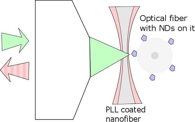
Figure 1: Procedure of single nanocrystal pickup onto optical fiber
Figure 2: Positioning on nanocrystals on nanostructures
Recent Publications
- Alexander Sushkov, Nicholas Chisholm, Igor Lovchinsky, Minako Kubo, Pik Kwan Lo, Steven Bennett, David Hunger, Alexey Akimov, Ronald L Walsworth, Hongkun Park, Mikhail D Lukin (2014) All-optical sensing of a single-molecule electron spin. Nano Lett., 14 (11): 6443–6448.
- Dmitry Sovyk, Victor Ralchenko, Maxim Komlenok, Andrew Khomich, Vladimir Shershulin, Vadim Vorobyev, Igor Vlasov, Vitaly Konov, and Alexey Akimov (2015) Fabrication of diamond microstub photoemitters with strong photoluminescence of SiV color centers:bottom-up approach. Applied Physics A, 118(1).
- M Y Shalaginov, V V Vorobyov, J Liu, M Ferrera, A V Akimov, A Lagutchev, A N Smolyaninov, V V Klimov, J Irudayaraj, A V Kildishev, A Boltasseva and V M Shalaev (2014) Enhancing the nanodiamond nitrogen-vacancy single‑photon source with TiN/AlScN hyperbolic metamaterial superlattice Laser Photonics Rev., 1–8.
- Vorobyov V V, Soshenko V V, Bolshedvorskii S V, Javadzade J, Lebedev N, Smolyaninov A N, Sorokin V N, Akimov A V (2016) Coupling of single NV center to adiabatically tapered optical single mode fiber. Eur. Phys. J. D 70(12): 269.
- Vorobyov V V, Kazakov A Y, Soshenko V V, Korneev A A, Shalaginov M Y, Bolshedvorskii S V, Sorokin V N, Divochiy A V, Vakhtomin Y B, et al (2017) Superconducting detector for visible and near-infrared quantum emitters. Opt. Mater. Express 7(2), 513.
Branislav Vlahovic
North Carolina Central University, USA
Title: Optical sensing for dynamics of the localized/delocalized states in binary quantum

Biography:
Branislav Vlahovic is Director of the National Science Foundation Computational Center of Research Excellence, NASA University Research Center for Aerospace Device, and NSF Center Partnership for Research and Education in Materials at North Carolina Central University. In 2004, he was awarded by the Board of Governors of The University System of North Carolina Oliver Max Gardner statewide award for his research and contribution to science. He has published more than 300 papers in peer-reviewed journals. His research interest includes pulsed laser deposition of nanostructures, nonlinear optics, computer simulations of nanostructures, tunneling and charge transfer between nanostructures, detectors and devices based on quantum confinement, nanophotonics, semiconductor structures and photovoltaics.
Abstract:
Weakly coupled binary nano-sized systems demonstrate perspectives for nano-sensor applications. We study electron/hole localization and spectral distributions of localized/delocalized states in binary InAs/GaAs quantum complexes, including quantum wells (QWs) and quantum dots (QDs). The InAs/GaAs heterostructures are described using the effective potential model. It was shown, that the electron tunneling and spectral distributions of localized/delocalized states in binary system is extremely sensitive on shape symmetry violations. The parameter![]() , which defines delocalized (
, which defines delocalized (![]() ) or localized (
) or localized (![]() 0) states of an electron, depends on the energy difference
0) states of an electron, depends on the energy difference ![]() of the spectra in left and right QDs. The difference can be caused by a shape symmetry violation. The sensitivity of the parameter
of the spectra in left and right QDs. The difference can be caused by a shape symmetry violation. The sensitivity of the parameter ![]() to the small variations of
to the small variations of ![]() is estimated as
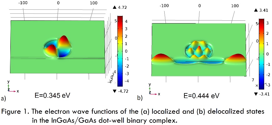
is estimated as ![]() . This work focuses on the optical registration of the localized/delocalized states dynamics. Modeling of carrier transfer from a barrier in InAs/GaAs dot-well, tunnel-injection structure is performed. In Fig 1, shown is the electron wave functions of the localized and delocalized states calculated for two spectral levels: E=0.345 eV and E=0.444 eV, respectively. The energy of the delocalized state corresponds to that one for which the tunneling between dot and well occurs. The relation to the PL experiments for such complexes is provided. We model the second pick of the PL spectrum, which corresponds to the carriers tunneling in the dot-well complex, in the terms of the localized/delocalized states. Influence of the variations of geometrical parameters of QD and QW on the tunneling will be presented.
. This work focuses on the optical registration of the localized/delocalized states dynamics. Modeling of carrier transfer from a barrier in InAs/GaAs dot-well, tunnel-injection structure is performed. In Fig 1, shown is the electron wave functions of the localized and delocalized states calculated for two spectral levels: E=0.345 eV and E=0.444 eV, respectively. The energy of the delocalized state corresponds to that one for which the tunneling between dot and well occurs. The relation to the PL experiments for such complexes is provided. We model the second pick of the PL spectrum, which corresponds to the carriers tunneling in the dot-well complex, in the terms of the localized/delocalized states. Influence of the variations of geometrical parameters of QD and QW on the tunneling will be presented.
Recent Publications
- Filikhin I, Karoui A and Vlahovic B (2016) Nanosensing Backed by the Uncertainty Principle. Journal of Nanotechnology. doi:10.1155/2016/3794109.
- Filikhin I, Suslov V M and Vlahovic B (2006) Modeling of InAs/GaAs quantum ring capacitance spectroscopy in the nonparabolic approximation. Phys. Rev. B 73: 205332-4.
- Filikhin I, Matinyan S G and Vlahovic B (2015) Electronic structure of quantum dots and rings. Reviews in Theoretical Science 3: 1-22.
- Filikhin I, Karoui A and B. Vlahovic B (2016) Single electron tunneling in double and triple quantum wells. International Journal of Modern Physics B 30: 1642011-9.
- Filikhin I, Matinyan S G and Vlahovic B (2015) Localized-delocalized states and tunneling in double quantum dots: effect of symmetry violation. Quantum Matter 4: 1-7.
H C Ong
The Chinese University of Hong Kong, Hong Kong
Title: Study of the angular momentum of light from plasmonic crystals

Biography:
H C Ong received his BA and PhD in Materials Science and Engineering from Northwestern University, USA. He currently is an Associate Professor in Physics Department, at the Chinese University of Hong Kong. He has been working on amorphous carbon, diamond, and ZnO for years and his current interest is light-matter interaction focusing on plasmonics. He has published more than 100 technical papers on fluorescence and sensing. He has been serving as an Organizer of international conferences.
Abstract:
In analogy to electron waves, electromagnetic waves also carry spin and orbital angular momentum (AM) and this property has been fascinating the world of optical science and engineering for many years. With the rise of nanotechnology, photonic systems can now be fabricated at the length scale of nanometers, manifesting many intriguing phenomena including the spin-orbit interaction in an observable extent. The polarization, the spatial field distribution, and the propagation direction are no longer treated separately and controlling one with another has become feasible. Plasmonic arrays are one of the most popular nanophotonic systems owing to their simplicity and well-defined structures for yielding controllable optical properties. They have been used in extraordinary transmission, fluorescence, photovoltaics, nonlinear optics, sensing, etc. In addition, since surface plasmon polaritons (SPPs) carry transverse spin AM, they should modify the AM of the outgoing radiation under the conservation of angular momentum. Unfortunately, this transverse spin is not properly taken into consideration even though plasmonic research has been carried out for years. Here, I will talk about the AM of light from plasmonic crystals. We have observed substantial polarization conversion and spin-orbital coupling from square lattice circular nanohole arrays, which do not possess intrinsic chirality. We find the transverse spin AM possessed by SPPs play a deterministic role in governing the far-field radiation. The experimental results are supported by finite-difference time-domain simulations and temporal coupled mode theory. Based on the AM study, we propose the AM can be used as a new parameter in surface plasmon resonance (SPR) sensing. As the transverse spin AM of SPPs is strongly dependent on the complex propagation wave vector, which is sensitive to the change of the local refractive index, the change in the AM of light thus reflects the sensing environment. The performance of the spin-SPR will be discussed.
Recent Publications
- Cao ZL, Yiu LY, Zhang ZQ, Chan CT, Ong HC (2017) Understanding the role of surface plasmon polaritons in two-dimensional achiral nanohole arrays for polarization conversion. Phys. Rev. B (in press).
- Lin M, Cao ZL, Ong HC (2017) Determination of the excitation rate of quantum dots mediated by momentum resolved Bloch-like surface plasmon polaritons. Opt. Exp. 25: 6092-6103.
- Cao ZL, Ong HC (2016) Momentum-dependent group velocity of surface plasmon polaritons in two-dimensional metallic nanohole array. Opt. Exp. 24: 12489-12500.
- Liu C, Chan CF, Ong HC (2016) Direct deconvolution of electric and magnetic responses of single nanoparticles by Fourier space surface plasmon resonance microscopy. Opt. Comm. 378: 28-34.
- Liu SD, Leong ESP, Li GC, Hou YD, Deng J, Teng JH, Ong HC, Lei DY (2016) Polarization-independent multiple fano resonances in plasmonic nonamers for multimode-matching enhanced multiband second-harmonic generation. ACS Nano 10: 1442-1452.
Jian Fu
Zhejiang University, China
Title: A possible approach to quantum computation by using classical optical fields modulated with pseudorandom phase sequence

Biography:
Jian Fu has completed his PhD at Zhejiang University. He is working as Associate Professor at Zhejiang University. He has published more than 45 papers in reputed journals.
Abstract:
The history to simulate quantum states using classical optical fields is long. Many researchers utilized classical optical fields to simulate quantum states and quantum computations. However, it is quickly found that the simulation is not efficient and scalable. This is because the classical optical field only supports the product structure but does not support tensor product structure. We proposed a possible scheme to solve the problem that optical ï¬elds modulated with pseudorandom phase sequences simulate any state of multiple quantum particles. By using the scheme, we demonstrated optical analogies to many quantum states such as Bell states, GHZ states and W states, and some quantum algorithms such as Shor’s algorithm, Grove’s algorithm and quantum Fourier Transformation. Firstly, we introduced a theoretical framework, a phase ensemble based on pseudorandom phase sequence referring from the concept of quantum ensemble. Then, we represented various quantum states of n particles by using classical fields modulated with n pseudorandom phase sequences and we also demonstrated nonlocal properties of quantum entanglement in the phase ensemble theoretical framework. Finally, we demonstrated some optical implementations to realize some quantum algorithms. We believe these optical implementations are not difficult to implement. After careful analysis and numerical simulation, we can conclude that our scheme provides an efficient approach to quantum computation without exponential classical resources.

Biography:
Jae Eun Jang received his PhD degree in Electrical Engineering from the University of Cambridge, UK in 2006. From 2007 to 2011, he was Principal Senior Researcher at Samsung Advanced Institute of Technology, Yongin, Korea. Since 2011, he has been a Professor in Information and Communication Engineering at Daegu Gyeongbuk Institute of Science and Technology (DGIST), Daegu, Korea. He first demonstrated the mechanical nanoswitch and mechanical DRAM concept using vertically aligned carbon nanotubes in 2004 and 2008, respectively. More recently he was involved in nanodevices for ultra-fast driving, biomimic concepts and brain-machine interface. He has authored or co-authored over 200 journal and conference papers, and is an inventor of 100 granted patents.
Abstract:
The different working principles of nano hole array structure from general color can make promising features as a bio-detector because the structural color filter (SCF) changes easily, the filtering colors by covering of different biomaterials. Because the nano-hole arrays were designed to present a filtered peak wavelength in the visible light region, filtered color changes caused by different biomolecules were easily observed with a microscope or even by the naked eye. Generally, many biomolecules are transparent or colorless in the visible range, so that it is hard to distinguish among them using visible observation. However, their molecular structure and composition induce some differences in the dielectric constant or refractive index, causing a filtered color shift in the nano-hole array structure. Here, the contribution of geometric parameters such as the hole diameter and the spacing between nano-holes for bio-detection was evaluated to maximize the change in color among different biomolecules. A larger hole size and space between the holes enabled the biomolecules to be easily distinguished. Even if the change in color was not distinctive enough by eye in some cases, it was possible to distinguish the change by simple analysis of the ‘Hue’ values or by the ‘Lab’ color coordinates obtained from the photo images. Therefore, this skill can have high probability of realization for real-time detection of cells without the use of bio-markers
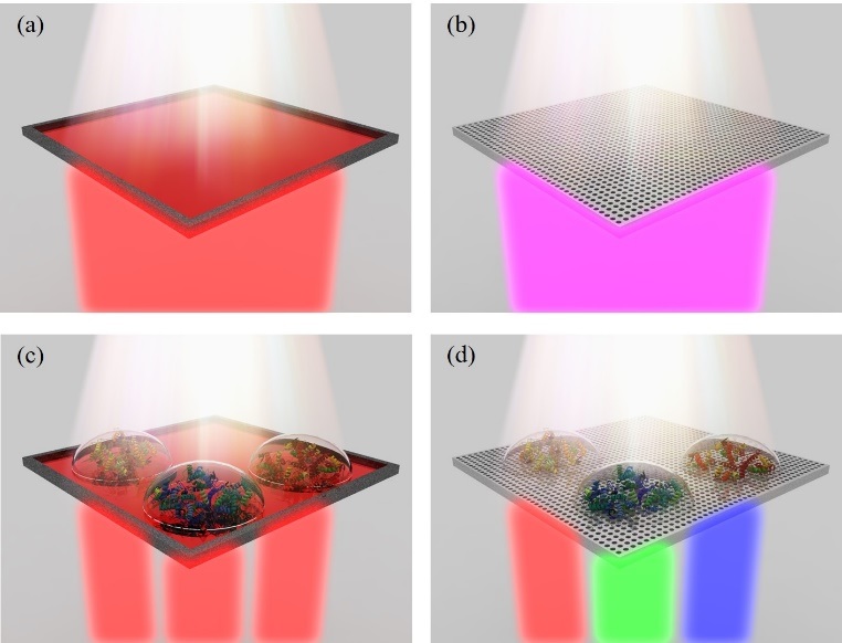
Figure 1: Concept images of bio-detection based on a SCF. (a) Image of a general red CF based on red pigments. Except for the red color component, the other components in white light are absorbed by the red pigments (b) Schematic image of a SCF. Nano-hole arrays induce a color filtering effect (c) Even though three different proteins are dropped on a general CF; there are no color changes due to its transparent optical property. (d) Different transparent biomolecules change the dielectric property of the surface of filters when they are dropped on the SCF. This causes spectral shifts in the SCF
Recent Publications
- M Ryu, et. al. (2017) Enhancement of interface characteristics of neural probe based on graphene, ZnO nanowires, and conducting polymer PEDOT. ACS Applied Materials & Interfaces. 9 (12): 10577–10586.
- M Sim et. al. (2016) Structural solution to enhance the sensitivity of a self-powered pressure sensor for an artificial tactile system. IEEE Transactions on Nanobioscience. 15: 804-811.
- J H Shin et. al. (2016) Ultrafast metal-insulator-multi-wall carbon nanotube tunneling diode employing asymmetrical structure effect. Carbon 102: 172-180.
- S Kim et. al. (2016) Geometric effects of nano-hole arrays for label free bio-detection. RSC Advances 6: 8935-8940.
- B O Jun et. al. (2015) Wireless thin film transistor based on micro magnetic induction coupling antenna. Scientific Reports 5:18621.
Johan Bauwelinck
Ghent University, Belgium
Title: High-speed transceiver electronics for next-generation optical networks

Biography:
Johan Bauwelinck received his PhD degree in Applied Sciences, Electronics from Ghent University, Belgium in 2005. Since Oct 2009, he is a Professor in the IDLab research group of the Department of Information Technology (INTEC) at the same university where he is leading the Design lab since 2014. He became a Guest Professor at iMinds in the same year, now IMEC since 2016. His research focuses on high-speed, high-frequency (opto) electronic circuits and systems, and their applications on chip and board level, including transmitter and receiver analog front-ends for wireless, wired and fiber-optic communication or instrumentation systems. He is an active person involved in the EU-funded projects GIANT, POWERNET, PIEMAN, EuroFOS, C3-PO, Mirage, Phoxtrot, Spirit, Flex5Gware, Teraboard, Streams, WIPE and Optima conducting research on advanced electronic integrated circuits for next generation transport, metro, access, datacenter and radio-over-fiber networks. He has promoted 18 PhDs and co-authored more than 200 publications and 10 patents in the field of High-Speed Electronics and Fiber-Optic Communications.
Abstract:
High-speed electronic integrated circuits are essential to the development of new fiber-optic communication systems. Exponentially increasing data consumption is expanding the applications of optical communication and driving the development of faster and more efficient transceivers. Fiber-optic communication networks operate on very different scales from very short interconnects in datacenters to very long links between cities, countries or continents. Optical fibers are also increasingly used for access networks (e.g. fiber-to-the-home) and for mobile fronthauling and backhauling. Advances in opto-electronic devices, high-volume manufacturing and packaging technologies are driving numerous developments in these diverse applications. Because of the increasing speeds, close integration and co- design of photonic and electronic devices have become a necessity to realize high-performance sub-systems, while such co-design brings new opportunities as well on the sub-system architecture level to break traditional performance-cost trade-offs. There is no single best solution among electrical and optical technologies due to the different technological constraints in terms of distance, footprint, power consumption, cost, etc. Research is approaching this challenge from different angles, with technological improvements on photonic and electronic devices and/or by applying more complex modulation and signal processing. While each application operates on a very different scale (fiber length, number of users) with very different requirements (capacity, signal format, cost, power, etc.), they share one thing, their need for application-specific high-speed electronic transceiver circuits such as driver amplifiers, transimpedance amplifiers, equalizers and clock-and- data recovery circuits. This presentation will illustrate a few recent and ongoing developments from various H2020 projects.
Figure 1: 56Gb/s PAM-4 single-mode VCSEL driver array
Figure 2: 64Gb/s PAM-4 transimpedance amplifier array
Recent Publications
- M Vanhoecke et. al. (2017) Segmented optical transmitter comprising a CMOS driver array and an InP IQMZM for advanced modulation formats. J. Lightw. Technol. 35(4):862- 867.
- J Verbist et. al. (2016) A 40-GBd QPSK/16-QAM integrated silicon coherent receiver. IEEE Photon. Technol. Lett. 28(19):2070-2073.
- B. Moeneclaey et. al. (2017) 40-Gb/s TDM-PON downstream link with Low-Cost EML transmitter and APD-Based electrical duobinary receiver. J. Lightw. Technol. 35(4):1083-1089.
Nikola Z Petrović
University of Belgrade, Serbia
Title: General analytic solutions to the various forms of the nonlinear Schrödinger equation using the Jacobi elliptic function expansion method

Biography:
Nikola Z Petrović received his BSc in Mathematics and in Physics at MIT (Massachusetts Institute of Technology) in 2003 and his PhD in Physics at University of Belgrade in 2013. He was employed as a Teaching Associate and Lab Coordinator at Texas A&M University at Qatar from 2005 to 2012. He is currently an Assistant Research Professor at Institute of Physics, Belgrade. His primary field of expertise is Mathematical Physics applied to nonlinear optics, in particular finding novel exact solutions to the nonlinear Schrodinger equation, the Gross-Pitaevskii equation and other related equations.
Abstract:
The advent of meta-materials has made materials with a negative refractive index possible. This has opened up a possibility of finding stable solutions to various nonlinear equations that naturally occur in the field of nonlinear optics through the use of dispersion management. Finding such stable solutions is invaluable for the field of photonics and has many potential practical applications. In our work we use the F-expansion method applied to the Jacobi elliptic function, along with the principle of harmonic balance to find novel solutions to various forms of the Nonlinear Schrödinger equation (NLSE). This approach allowed us to assume a quadratic form for the phase with respect to the longitudinal variable and thus find solutions both with and without chirp. Earlier work done on the NLSE with Kerr nonlinearity, with both normal and anomalous dispersion, was generalized to nonlinearities of arbitrary polynomial nonlinearity. Stable solutions were also obtained for the Gross-Pitaevskii equation. These solutions were determined to be modulationally stable, either unconditionally or with dispersion management, depending on the signs of various parameters in the original equation. The method was subsequently generalized for functions satisfying an arbitrary elliptic differential equation, including Weierstrass elliptic functions. A relatively new line of research has been finding solutions to the NLSE in a parity-time (PT) conserving potential, i.e. one for which the real part is an even function and the complex part is an odd function. We found a rich new class of exact solutions where the potential resembles the Scarf II potential.

Figure 1: Solution to the NLSE with Kerr nonlinearity using the Weierstrass elliptic function described in: (a) without chirp (b) with chirp
- S L Xu, Y Zhao, N Z Petrović and M R Belić (2016) Spatiotemporal soliton supported by parity-time symmetric potential with competing nonlinearities. Europhysics Letters. 115: 14006.
- N Z Petrović and M Bohra (2016) General Jacobi elliptic function expansion method applied to the generalized (3+1)-dimensional nonlinear Schrödinger equation. Optical and Quantum Electronics. 48: 1-8.
- S L Xu, N Petrović, M R Belić and W Deng (2016) Exact solutions for the quintic nonlinear Schrödinger equation with time and space. Nonlinear Dynamics 84: 251.
- N Z Petrović, N B Aleksić and M R Belić (2015) Modulational stability analysis of exact multidimensional solutions to the generalized nonlinear Schrödinger equation and the Gross-Pitaevskii equation using a variational approach. Optics Express 23: 10616.
- W P Zhong, L Chen, M R Belić and N Petrović (2014) Controllable parabolic-cylinder optical rogue wave. Physical Review E. 90: 043201.
V A Belyakov
Landau Institute for Theoretical Physics, Russia
Title: Optics of photonic liquid crystals at frequencies of localized modes

Biography:
V A Belyakov graduated from Moscow Engineering Institute in 1961 and was a Postgraduate student of I V Kurchatov Atomic Energy Institute during 1961–64. He received Doctor of Science degree in 1974. He was the Head of Laboratory in All-Union Physics-Technical and Radio–Technical Institute from 1964 to 1982 and Surface and Vacuum Research Centre, Moscow during 1982–1995. Since 1995, he is a Senior Researcher in L D Landau Institute for Theoretical Physics. Since 1982, he is a Part-time Professor in Moscow Institute for Physics and Technology; and short term Visiting Professor of some universities: Leuven (Belgium), Tokyo (Japan), Paris Sud (France), Glasgow Thrathclyde (Scotland), etc. He is the Author of the following monographs: Optics of Cholesteric Liquid Crystals, 1982, Optics of Chiral Liquid Crystals, 1989; Diffraction Optics of Complex Structured Periodic Media , 1988, 1992; Optics of Photonic Crystals, Publishing House of Moscow Institute of Physics and Technology, 2013 (Textbook, in Russian). He is honored with the Grants of Russian Foundation for Basic Research (RFBR), Soros Grants, and INTAS Grants. He is a Member of Russian Academy of Natural Sciences, Member of Russian Academy of Metrology, Member of International Liquid Crystal Society and Liquid Crystal Society of CIS (member Governing body 1982).
Abstract:
Recently great attention was paid to the localized optical modes in photonic crystals, in particular, in photonic liquid crystals due to their efficient application in the linear and nonlinear optics. Here a brief survey of the publications and original theoretical results on the localized optical modes in photonic liquid crystals in connection with explanation of the corresponding experimental observations are presented. Theoretical studies were performed for the certainty, as the example of chiral liquid crystals (CLCs). The chosen model (absence of dielectric interfaces in the studied structures) allows one to get rid off the polarization by mixing at the surface of the CLC layer and the defect structure (DMS) to reduce the corresponding equations to equations for the light of diffraction in the CLC polarization, to obtain an analytic description of localized edge (EM) and defect (DM) modes. The dispersion equations determining connection of the EM and DM frequencies with the CLC layer parameters and other parameters of the DMS are obtained. Analytic expressions for the transmission and reflection coefficients of the DMS are presented and analyzed. Specific cases were considered, as DMS with an active (i.e. transforming the light intensity or polarization) defect layer, CLC layer of local anisotropic absorption and conic-helical director structures. It is shown that the active layer (excluding an amplifying one) reduces the DM life-time (and increase the lasing threshold) in comparison with the case of DM at an isotropic defect layer. The case of CLC layers with an anisotropic local absorption is also analyzed and, in particular, shown that due to the Borrmann effect the EM life-times for the EM frequncies at the opposite stop-bands edges may be signifinately different and so in the experiment optimization of it should be taken into account. The experimentally observed enhancement of some optical effects in photonic liquid crystals at the EM and DM frequencies (lowering of the lasing threshold, abnormally strong absorption, etc.) are in good agreement with the presented theory. Options of experimental observations of the new theoretically revealed phenomena are discussed. It is emphasized that the presented localized modes in CLC results are of a general nature and are qualitatively applicable for the localized modes in other structures.
REFERENCES
- Liquid Crystals Microlasers, Eds. L.M.Blinov, R.Bartolino, Transword Research Network, 2010.
- V. I. Kopp, Z.-Q. Zhang, and A. Z. Genack, Prog. Quantum Electron. 27, 369 (2003).
- V.A.Belyakov, S.V,Semenov, JETP , 118, 798 (2014).
- V. A. Belyakov, Mol. Cryst. Liquid Cryst. 612, 81 (2015).
Enayet Rahman
University of London, UK
Title: Optical waveguide properties of myelinated and unmyelinated nerve axons from ultraviolet to NIR wavelengths

Biography:
Abstract:
Statement of the Problem: Infrared Nerve Stimulation (INS) is becoming popular because of its potential to provide targeted stimulation. Recently it was claimed that myelin sheath can guide light (200 nm – 1300 nm), however propagation characteristics were not reported for wavelengths l > 1500 nm, common in INS. We present them here for l up to 2000 nm for both myelinated and unmyelinated nerve fibers.
Methodology & Theoretical Orientation: Modal analysis was performed on the cross-section of the nerve fiber by solving Maxwell’s equations. The effective index (n_eff) of the first three modes was determined and the single mode operating wavelength range was determined for both myelinated and unmyelinated nerve fibers, using a 4-um diameter axon. The overall diameter of the myelinated fiber was 6.66 um. The refractive indices of the fiber cytoplasm, the myelin sheath, and the outside medium were set as 1.34, 1.44 and 1.38 respectively.
Findings: The optical power propagating through unmyelinated fiber is confined by the index of the fiber’s cytoplasm (1.38) being higher than its surrounding (1.34). The effective indices of the first three propagating modes were determined and plotted in for 200nm ≤ l ≤ 2000nm. It was found that the unmyelinated fiber is single-mode for l > 1700 nm. In the myelinated fiber, optical power is confined within the myelin sheath (1.44). The effective indices of the myelinated fiber indicate that it supports more modes than the unmyelinated one and the myelin sheath operates in a single-mode condition for wavelengths longer than 1980 nm. This article determines light propagation characteristics of nerve fibers for a range of wavelengths, making it very useful for future INS designs. This study can also be useful in the field of interfacing brain using light.